Chapter 6 Solids And Semiconductors Devices Multiple Choice Questions
Question 1. Symbolic representation of photodiode is-

Answer: 1.
Question 2. Symbol of Zener diode-
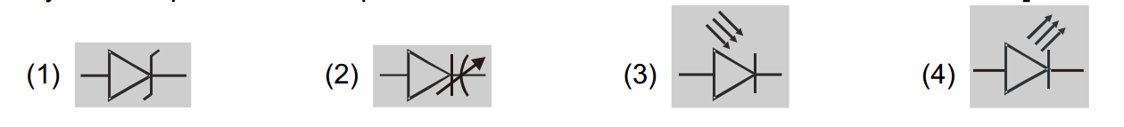
Answer: 1.
Question 3. The diffusion current in a p-n junction is greater than the drift current in magnitude
- If The Junction is forward-biased
- If The Junction is reverse-biased
- If The Junction is unbiased
- In No Case
Answer: 1. If The Junction is forward-biased
Question 4. In a p-n junction,
- New Holes And Conduction Electrons Are Produced Continuously Throughout The Material
- New Holes And Conduction Electrons Are Produced Continuously Throughout The Material Except In The Depletion Region
- Holes And Conduction Electrons Recombine Continuously Throughout The Material.
- Holes And Conduction Electrons Recombine Continuously Throughout The Material Except In The Depletion Region.
Answer: 1. New Holes And Conduction Electrons Are Produced Continuously Throughout The Material
Question 5. A hole diffuses from the p-side to the n-side in a p-n junction. This means that
- A Bond Is Broken On The N-Side And The Electron Freed From The Bond Jumps To The Conduction Band
- A Conduction Electron On The P-Side Jumps To A Broken Bond To Complete It
- A Bond Is Broken On The N-Side And The Electron Freed From The Bond Jumps To A Broken Bond On The P-Side To Complete It
- A Bond Is Broken On The P-Side And The Electron Freed From The Bond Jumps To A Broken Bond On The N-Side To Complete It.
Answer: 3. A Bond Is Broken On The N-Side And The Electron Freed From The Bond Jumps To A Broken Bond On The P-Side To Complete It
Question 6. The depletion region of a P-N diode, under open circuit conditions, contains-
- Electrons
- Holes
- Unmasked immobile impurity ions
- Impurity atoms
Answer: 3. Unmasked immobile impurity ions
Question 7. A semiconducting device is connected in a series circuit with a battery and a resistance. A current is found to pass through the circuit. If the polarity of the battery is reversed, the current drops to almost zero. The device may be
- An Intrinsic Semiconductor
- A P-Type Semiconductor
- An N-Type Semiconductor
- A P-N Junction
Answer: 4. A P-N Junction
Question 8. Which is the wrong statement in the following sentence? A device in which P and N-type semiconductors are used is more useful than a vacuum tube because-
- Power Is Not necessary to Heat The Filament
- It Is More Stable
- Very little heat Is Produced In It
- Its Efficiency Is High Due To A High Voltage Drop Across The Junction
Answer: 4. Its Efficiency Is High Due To A High Voltage Drop Across The Junction
Question 9. When the value of current increases in P-N junction, then the value of contact potential-
- Decrease
- Increase
- Remain Unchanged
- Depends On Temperature
Answer: 1. Decrease
Question 10. The contact potential at the junction site in a P-N junction is-
- Positive On the P Side And Negative On the N Side
- Negative On the P Side And Positive On the N Side
- Zero
- Infinite
Answer: 2. Negative On the P Side And Positive On the N Side
Question 11. If V A and VB denote the potentials of A and B, then the equivalent resistance between A and B in the adjoint electric circuit is
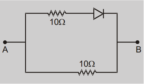
- 10 ohm if VA > VB
- 5 ohm if VA < VB
- 5 ohm if VA > VB
- 20 ohm if VA > VB
Answer: 3. 5 ohm if VA > VB
Question 12. In which case is the juction diode is not reverse bias-

Answer: 2.
Question 13. The depletion layer in the P-N junction is caused by
- Drift holes
- Diffusion of free carriers
- Migration of impurity ions
- Drift of electrons
Answer: 2. Diffusion of free carriers
Question 14. What accounts for the flow of charge carriers in forward and reverse biasing of silicon P-N diode-
- Drift in both reverse and forward bias
- Drift in forward bias and diffusion in reverse bias
- Drift in reverse bias and diffusion in forward bias
- Diffusion in both forward and reverse bias
Answer: 3. Drift in reverse bias and diffusion in forward bias
Question 15. The current flowing through the zener diode in fig. is-
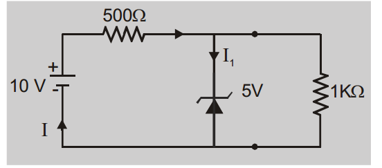
- 20 MA
- 25mA
- 15mA
- 5mA
Answer: 4. 5mA
Question 16. The resistance of a reverse baised P-N junction diode is about-
- 1 ohm
- 102 ohm
- 103 ohm
- 106 ohm
Answer: 4. 106 ohm
Question 17. Current I in the circuit shown will be
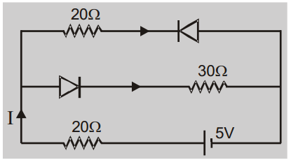
- \(\frac{5}{40}\)
- \(\frac{5}{50}\)
- \(\frac{5}{10}\)
- \(\frac{5}{20}\)
Answer: 2. \(\frac{5}{50}\)
Question 18. The value of barrier potential of P-N junction or N-P junction in Ge is-
- 0.03 volt in the direction of the forward current
- 0.3 volt in the direction opposite of the forward current
- 25 volts in the direction opposite to the forward current
- 25 volts in the direction of the forward current
Answer: 2. 0.3 volt in the direction opposite of the forward current
Question 19. The diffusion current in a P-N junction is greater than the drift current in magnitude-
- If The Junction is forward-biased
- If The Junction is reverse-biased
- If The Junction is unbiased
- In No Case
Answer: 1. If The Junction is forward-biased
Question 20. The barrier potential in a P-N junction is maximum in
- The Reverse Bias Condition
- The Forward Bias Condition
- The Condition When The Junction Diode Is Used As Rectifier
- Zero Bias Condition
Answer: 1. The Reverse Bias Condition
Question 21. The diffusion current in a P-N junction is-
- From The N-Side To The P-Side
- From The P-Side To The N-Side
- From The N-Side To The P-Side If The Junction Is Forward-Biased And In The Opposite Direction If It Is Reverse Baised
- From The P-Side To The N-Side If The Junction Is Forward-Biased And In The Opposite Direction If It Is Reverse Biased
Answer: 2. From The P-Side To The N-Side
Question 22. When a P-N diode is reversed biased, then the current through the junction is mainly due to
- Diffusion Of Charge
- Nature Of The Material
- Drift Of The Charges
- Both Drift And Diffusion Of The Charges
Answer: 3. Drift Of The Charges
Question 23. The drift current in a P-N junction is-
- From The N-Side To The P-Side
- From The P-Side To The N-Side
- From The N-Side To The P-Side If The Junction Is Forward-Biased And In The Opposite Direction If It Is reverse-biased.
- From The P-Side To The N-Side If The Junction Is Forward-Baised And In The Opposite Direction If It Is Reverse Baised.
Answer: 1. From The N-Side To The P-Side
Question 24. For a reverse bias P-N junction-
- P region is positive and current is due to electrons
- P region is positive and the current is due to holes
- P region is negative and the current is due to electrons
- P region is negative and current is due to both electrons and holes
Answer: 4. P region is negative and current is due to both electrons and holes
Question 25. In the P-N junction when do electron and holes stops moving from P to N and N to P-
- Increase in +ve and –ve ions at junction
- Increase in electron at junction
- Increase in holes at the junction
- Increase in holes and electrons at the junction
Answer: 1. Increase in +ve and –ve ions at junction
Question 26. The depletion layer in the silicon diode is 1m wide and the knee potential is 0.6 V, then the electric field in the depletion layer will be
- Zero
- 0.6 Vm–1
- 6 × 10⁴ V/m
- 6 × 10⁵ V/m
Answer: 4. 6 × 10⁵ V/m
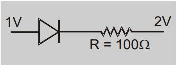
Question 27. The current through an ideal PN-junction shown in the following circuit diagram will be
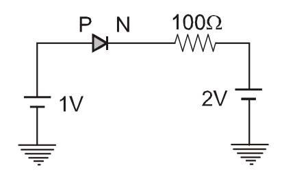
- Zero
- 1MA
- 10mA
- 30mA
Answer: 1. Zero
Question 28. In the circuit given below, the value of the current is
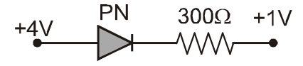
- 0amp
- 10-2 amp
- 1 amp
- 0.10 amp
Answer: 2. 10-2 amp
Question 29. The maximum efficiency of a full wave rectifier is
- 100 %
- 25.20 %
- 40.2 %
- 81.2 %
Answer: 4. 81.2 %
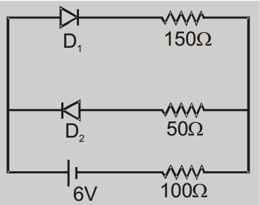
Question 30. The circuit shown in the figure contains two diodes each with a forward resistance of 50 ohm and infinite reverse resistance. If the battery voltage is 6V, find the current through the 100 ohm resistance.
- 0.01 Al
- 0.05A
- 0.2A
- 0.3A
Answer: 3. 0.2A
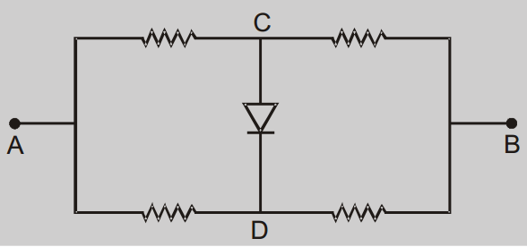
Question 31. Four equal resistors, each of resistance 10 ohm are connected as shown in the adjoining circuit diagram. Then the equivalent resistance between points A and B is
- 40 OHM
- 20ohm
- 10ohm
- 5 ohm
Answer: 3. 5 ohm
Question 32. In the arrangement shown in fig., the current through the diode is
- 10mA
- 1mA
- 20mA
- Zero
Answer: 4. Zero
Question 33. If the forward voltage in a semiconductor diode is changed from 0.5V to 2V, then the forward current changes by 1.5 mA. The forward resistance of the diode will be
- 1KΩ
- 2KΩ
- 4KΩ
- 8KΩ
Answer: 1. 1KΩ
Question 34. When the reverse potential in a semiconductor diode is 10V and 20V, the corresponding reverse currents are 25µA and 50µA respectively. The reverse resistance of the junction diode will be
- 40
- 4×10⁵
- 40k
- 4×10⁻⁵
Answer: 2. 4×10⁵
Question 35. A piece of copper and another of germanium are cooled from room temperature to 77 K, the resistance of:
- Each Of Them Increases
- Each Of Them Decreases
- Copper Decreases And Germanium Increases
- Copper Increases And Germanium Decreases
Answer: 3. Copper Decreases And Germanium Increases
Question 36. The electrical conductivity of a semiconductor increases when electromagnetic radiation of a wavelength shorter than 2480 nm, is incident on it. The band gap in (eV) for the semiconductor is :
- 1.1 eV
- 2.5 eV
- 0.5 eV
- 0.7 eV
Answer: 3. 0.5 eV
Question 37. If the ratio of the concentration of electrons to that of holes in a semiconductor is 5 and the ratio of 7 currents is 4, then what is the ratio of their drift velocities?
- 5/8
- 4/5
- 5/4
- 4/7
Answer: 3. 5/4
Question 38. If the lattice constant of this semiconductor is decreased, then which of the following is correct?

- All EC, Eg, Ev increase
- EC and EV increase, but EG decreases
- Ec and Ev decrease, but Eg increases
- All EC, Eg, Ev decrease
Answer: 3. Ec and Ev decrease, but Eg increases
Question 39. Carbon, silicon, and germanium have four valence electrons each. At room temperature which one of the following statements is most appropriate?
- The Number Of Free Conduction Electrons Is Significant In C But Small In Si And Ge
- The Number Of Free Conduction Electrons Is Negligibly Small In All The Three.
- The Number Of Free Electrons For Conduction Is Significant In All The Three.
- The number of free electrons for conduction is significant only in Si and Ge but is small in C.
Answer: 4. The Number Of Free Electrons For Conduction Is Significant Only In Si And Ge But Small In C.
Question 40. In A Crystal, The Atoms Are Located At The Position Of :
- Maximum Potential Energy
- Minimum Potential Energy
- Zero Potential Energy
- Infinite Potential Energy
Answer: 2. Minimum Potential Energy
Question 41. The Laptop Pc’s Modern Electronic Watches And Calculators Use The Following For Display:
- Single Crystal
- Poly Crystal
- Liquid Crystal
- Semiconductors
Answer: 3. Liquid Crystal
Question 42. A P-Type Semiconductor Is
- Positively Charged
- Negatively Charged
- Uncharged
- Uncharged At 0 K But Charged At Higher Temperatures.
Answer: 3. Uncharged
Question 43. In good conductors of electricity, the type of bonding that exists is :
- Ionic
- Vander Waals
- Covalent
- Metallic
Answer: 4. Metallic
Question 44. Bonding is a germanium crystal (semi-conductor) is:
- Metallic
- Ionic
- Vander Waal’s type
- Covalen
Answer: 4. Covalen