
Semiconductor Device MCQs For NEET
NEET Physics For Semiconductor Electronics: Materials, Devices, And Simple Circuits Multiple Choice Questions
Question 1. Sodium has body-centered packing. The distance between the two nearest atoms is 3.7Å. The lattice parameter is:
- 6.8Å
- 4.3 Å
- 3.0Å
- 8.6Å.
Answer: 2. 4.3 Å
We have, a neighbor distance of a body-centered cubic cell
d=\(\frac{\sqrt{3}}{2}\) a,
where a is the lattice parameter.
3.7=\(\frac{\sqrt{3 a}}{2}\)
a=\(\frac{2 \times 3.7}{\sqrt{3}}=4.3 Å\)
Question 2. Choose the only false statement from the following:
- In conductors, the valence and the conduction bands overlap.
- Substances with an energy gap of the order of 10 eV are insulators.
- The resistivity of a semiconductor increases with an increase in temperature.
- The conductivity of a semiconductor increases with an increase in temperature.
Answer: 3. The resistivity of a semiconductor increases with an increase in temperature.
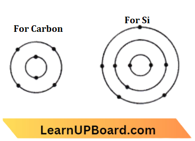
Question 3. Carbon, silicon, and germanium atoms have four valence electrons each. Their valence and conduction bands are separated energy band gaps represented \(\left(E_g\right)_c,\left(E_g\right)_{s i}\), and \(\left(E_g\right)_{G e}\) respectively. Which one of the following relationships is true in their case?
- \(\left(\mathrm{E}_g\right)_C>\left(\mathrm{E}_g\right)_{S i}\)
- \(\left(\mathrm{E}_g\right)_C<\left(\mathrm{E}_g\right)_{S i}\)
- \(\left(\mathrm{E}_g\right)_C=\left(\mathrm{E}_g\right)_{S i}\)
- \(\left(\mathrm{E}_g\right)_C>\left(\mathrm{E}_g\right)_{G e}\)
Answer: 1. \(\left(\mathrm{E}_g\right)_C>\left(\mathrm{E}_g\right)_{S i}\)
The band gap of carbon is 5.5 V while that of silicon is 1.1
∴ \(\mathrm{eV}\left(E_g\right)_C>\left(E_B\right)_S\)
Read and Learn More NEET Physics MCQs
Question 4. In semiconductors at room temperature:
- The valence band is partially empty and the condition band is partially filled
- The valance band is completely filled and the condition band is partially filled
- The valence band is completely filled
- The conduction band is completely empty.
Answer: 3. The valence band is completely filled
In semiconductors at room temperature, the valence band is partially empty and the conductor band is partially filled.
Semiconductor Device MCQs for NEET
Question 5. In the bcc structure of lattice constant a, the minimum distance between atoms is:
- \(\frac{\sqrt{3}}{2} \mathrm{a}\)
- \(\sqrt{2 \mathrm{a}}\)
- \(\frac{\mathrm{a}}{\sqrt{2}}\)
- \(\frac{a}{2}\)
Answer: 1. \(\frac{\sqrt{3}}{2} \mathrm{a}\)
In a bcc structure, the position vectors of the nearest neighbors are \(\left( \pm \frac{\mathrm{a}}{2} \hat{\mathrm{i}}, \pm \frac{\mathrm{a}}{2} \hat{\mathrm{j}}, \pm \frac{\mathrm{a}}{2} \hat{\mathrm{k}}\right)\).
In bcc, there will be atoms at the body center and at corners. So the distance between the two nearest atoms is
∴ \(\sqrt{\left(\frac{\mathrm{a}}{2}\right)^2+\left(\frac{\mathrm{a}}{2}\right)^2+\left(\frac{\mathrm{a}}{2}\right)^2}=\sqrt{\left(\frac{3 \mathrm{a}^2}{4}\right)}=\frac{\sqrt{3}}{2} \mathrm{a}\)
Question 6. Si and Cu are cooled to a temperature of 300K, then resistivity:
- For Si increases and for Cu decreases.
- For Cu increases and Si decreases.
- Decreases for both Si and Cu.
- Increases for both Si and Cu.
Answer: 1. For Si increases and for Cu decreases.
Due to the positive temperature coefficient, metal resistivity is directly proportional to temperature, but due to the negative temperature coefficient, the semiconductor resistivity is inversely proportional to temperature. It means that as temperature drops, metal resistivity drops but semiconductor resistivity rises. Si is a semiconductor, whereas Cu is a metal, in this case. As a result, Si resistivity increases while Cu resistivity falls.
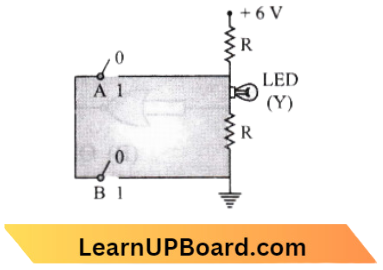
Question 7. C and Si both have the same lattice structure, having 4 bonding electrons in each. However, C is an insulator whereas Si is an intrinsic semiconductor. This is because:
- In the case of C, the valence band is not completely filled at absolute zero temperature.
- In the case of C, the conduction band is partly filled even at absolute zero temperature.
- The four bonding electrons in the case of C lie in the second orbit, whereas in the case of Si they lie in the third.
- The four bonding electrons in the case of C lie in the third orbit, whereas for Si they lie in the fourth orbit.
Answer: 3. The four bonding electrons in the case of C lie in the second orbit, whereas in the case of Si, they lie in the third.
Tetravalent atom → C , Si , Ge , Sn
Their outermost shell has four electrons
In Si, electrons have a loosely bond but in C, they tightly bond. Therefore C is used.
Question 8. The electron concentration in an n-type semiconductor is the same as the hole concentration in a p-type semiconductor. An external field (electric) is applied across each of them. Compare the currents in them:
- Current in n-type = current in p-type
- Current in p-type > current in n-type
- Current in n-type > current in p-type
- No current will flow in p-type, current will only flow in n-type.
Answer: 1. Current in n-type = current in p-type
Given
The electron concentration in an n-type semiconductor is the same as the hole concentration in a p-type semiconductor. An external field (electric) is applied across each of them.
Since electron and hole concentrations are the same, applying the same field will give the same current.
Semiconductor Device MCQs for NEET
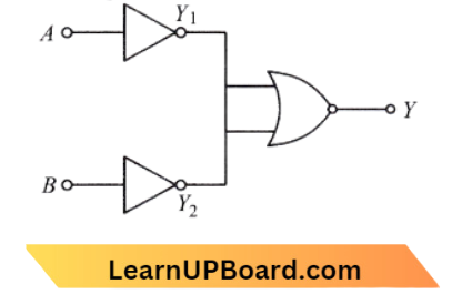
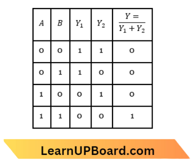
Question 9. An intrinsic semiconductor is converted into an n-type extrinsic semiconductor by doping it with
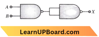
- Phosphorous
- Aluminium
- Silver
- Germanium.
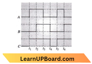
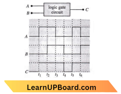
Answer: 1. Phosphorous
For an n-type semiconductor pentavalent impurity is needed and this is phosphorous.
Question 10. For a p-type semiconductor, which of the following statements is true?
- Holes are the majority carriers and trivalent atoms are the dopants.
- Holes are the majority carriers and pentavalent atoms are the dopants.
- Electrons are the majority carriers and pentavalent atoms are the dopants.
- Electrons are the majority carriers and trivalent atoms are the dopants.
Answer: 1. Holes are the majority carriers and trivalent atoms are the dopants.
p-type Semi-Conductor: To prepare a p-type semiconductor, a trivalent impurity with Si and G. Such an impurity atom wants to accept an electron from the crystal lattice. Thus effectively each dopant atom provides a hole. Thus holes are the majority carriers penta valent atoms are the dopants.
Question 11. In a n-type semiconductor, which of the following statement is true?
- Electrons are majority carriers and trivalent atoms are dopants
- Electrons are minority carriers and pentavalent atoms are dopants
- Holes are minority carriers and pentavalent atoms are dopants
- Holes are majority carriers and trivalent atoms are dopants
Answer: 3. Holes are minority carriers and pentavalent atoms are dopants
n-type semiconductors can be obtained by doping impurities such as pentavalent atoms (phosphores) etc.
MCQs on Semiconductor Devices for NEET
Question 12. If a small amount of antimony is added to the germanium crystal
- The antimony becomes an acceptor atom.
- There will be more free electrons than holes in the semiconductor.
- Its resistance is increased
- It becomes a p-type semiconductor.
Answer: 2. There will be more free electrons than holes in the semiconductor.
By adding pentavalent impurity only n-type semiconductors are constructed.
Question 13. Pure Si at 500 K has an equal number of electron (ne) and hole (nh) concentrations of 1.5 x 10¹⁶ m-3, Doping by indium increases nh to 4.5 x 10²² m-3. The doped semiconductor is of:
- n-type with electron concentration \(n_e=5 \times 10^{22} \mathrm{~m}^{-3}\)
- n-type with electron concentration \(n_e=2.5 \times 10^{10} \mathrm{~m}^{-3}\)
- n-type with electron concentration \(n_e=2.5 \times 10^{23} \mathrm{~m}^{-3}\)
- n-type with electron concentration \(n_e=5 \times 10^9 \mathrm{~m}^{-3}\)
Answer: 4. n-type with electron concentration \(n_e=5 \times 10^9 \mathrm{~m}^{-3}\)
See the question,\(n_i{ }^2 =n_e n_n\)
⇒ \(n_e =\frac{\left(n_i\right)^2}{n_n}=\frac{\left(1.5 \times 10^{16}\right)^2}{4.5 \times 10^{22}}\)
⇒ \(\left\{\right. Here n_i=1.5 \times 10^{16} and \left.n_n=4.5 \times 10^{22}\right\}\)
⇒ \(n_e=5 \times 10^9 \mathrm{~m}^{-3}\)
∴ \(n_n \gg n_e\) The semi-conductor is p-type.
Question 14. In the energy band diagram of a material shown below, the open circles and filled circles denote holes and electrons respectively. The material is:
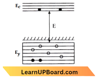
- An insulator
- A metal
- An u-type semiconductor
- A p-type semiconductor.
Answer: 4. A p-type semiconductor.
That material is a p-type semiconductor.
MCQs on Semiconductor Devices for NEET
Question 15. When arsenic is added as an impurity to silicon, the resulting material is:
- u-type semiconductor
- p-type semiconductor
- u-type conductor
- Insulator.
Answer: 1. u-type semiconductor
An n-type semiconductor is formed when a small amount of pentavalent impurity is added to a pure semiconductor. Arsenic (33) is the Pentavalent impurity. The presence of a pentavalent impurity in the semiconductor crystal results in a large number of free electrons.
Question 16. The increase in the width of the depletion region in a p-n junction diode is due to:
- Reverse bias only
- Both forward bias and reverse bias
- Increase in forward current
- Forward bias only.
Answer: 1. Reverse bias only
A p-n Junction diode is formed by fusing one p-type and one n-type. This happens because when substrate we apply reverse bias voltage, the electrons drift away from the junction and hence conduction is not possible. So, the width of the depletion region in a p-n junction diode is increased by reverse bias.
Question 17. In an unbiased p-n junction holes from the p-region to the n-region because of:
- The attraction of the free electrons of the n-region.
- The higher hole concentration in the p-region than that in the n-region.
- The higher concentration of electrons in the n-region than that in the p-region.
- The potential difference across the p-n junction.
Answer: 2. The higher hole concentration in the p-region than that in the n-region.
Question 18. In forward biasing of the p-n junction:
- The positive terminal of the battery is connected to the n-side and the depletion region becomes thin
- The positive terminal of the battery is connected to the n-side and the depletion region becomes thick
- The positive terminal of the battery is connected to the p-side and the depletion region becomes thin
- The positive terminal of the battery is connected to the p-side and the depletions region becomes thick.
Answer: 3. The positive terminal of the battery is connected to the p-side and the depletion region becomes thin
In forward biasing, the width of the deption layer is decreased.
Question 19. Application of a forward bias to a p-n junction:
- Widens the depletion zone
- Increases the potential difference across the depletion zone
- Increases the number of donors on the N-side
- Decreases the electric field in the depletion zone.
Answer: 4. Decreases the electric field in the depletion zone.
Forward biased to p-n Junction decreases the electric field in the depletion zone
Semiconductor Questions NEET
Question 20. In ap-n junction:
- High potential is at the n-side and low potential at the p-side
- High potential is at the p-side and low potential at the n-side
- P and both are at the same potential
- Undetermined.
Answer: 1. High potential is at the n-side and low potential at the p-side
In a p-n junction high potential is at w-side and law potential at p-side.
Question 21. The depletion layer in the p-n junction region is caused by:
- Drift of holes
- Diffusion of charge carriers
- Migration of impurity ions
- Drift of electrons.
Answer: 2. Diffusion of charge carriers
When a p-n junction is formed, some of the free electrons in the n region diffuse across the junction and combine with holes to form negative ions. In doing so, they leave behind positive ions at the donor impurity sites. Similarly, holes from the p side diffuse to the n side and thus form a layer called diffusion layer at the junction.
So, the depletion region is caused by the diffusion of charge carriers.
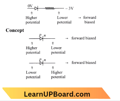
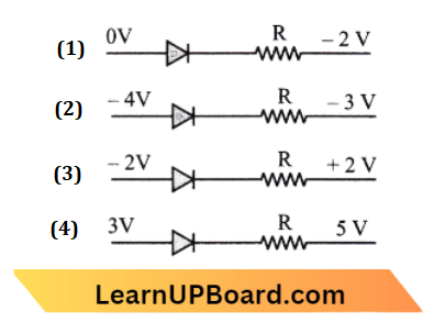
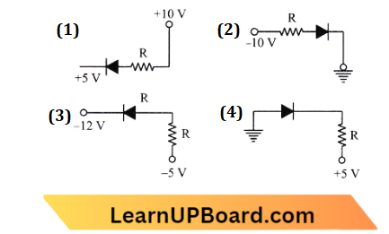
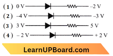
Question 22. Out of the following which one is a forward-biased diode?
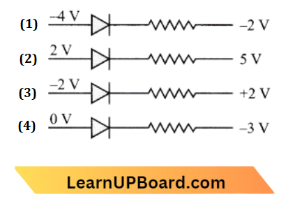
Answer: 4.
Semiconductor Questions NEET
Question 23. In a p-n junction diode, change in temperature due to heating:
- Does not affect the resistance of the p-n junction
- Affects only forward resistance
- Affects only reverse resistance
- Affects the overall V-I characteristics of the p-n junction.
Answer: 4. Affects the overall V-I characteristics of the p-n junction.
Due to heating, the number of electron-hole pairs will increase. So, the overall resistance of the diode will change. Due to this forward biasing and reverse biasing both are changed.
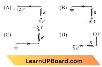
Question 24. Which one of the following represents the forward bias diode?
Answer: 1.
In forward bias, the p-type semiconductor is at higher potential w.r.t. n-type semiconductor, and in reverse bias p – type semiconductor is at lower potential w.r.t. p-type semiconductor.
Semiconductor Questions NEET
Question 25. Consider the junction diode as ideal. The value of current flowing through AB is:
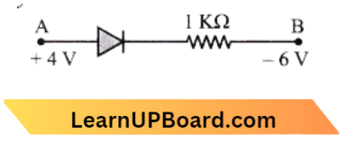
- \(10^{-2} \mathrm{~A}\)
- \(10^{-1} \mathrm{~A}\)
- \(10^{-3} \mathrm{~A}\)
- \(0 \mathrm{~A}\)
Answer: 1. \(10^{-2} \mathrm{~A}\)
Current, I =\(\frac{V_A-V_B}{R} \)
since V=I R
= \(\frac{4-(-6)}{1 \mathrm{~K} \Omega}=\frac{10}{1 \times 10^3}=10^{-2} \mathrm{~A}\)
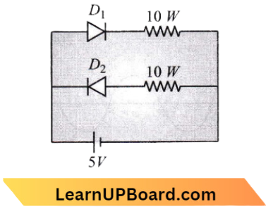
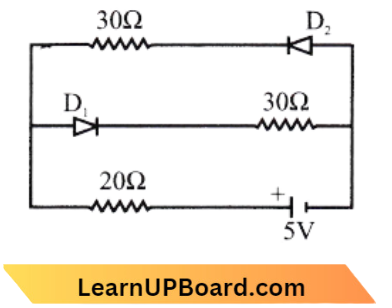
Question 26. The given circuit has two ideal diodes connected as shown in the figure below. The current flowing through the resistance R1 will be:
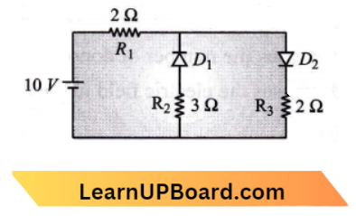
- 2.5 A
- 10.0 A
- 1.43 A
- 3.13 A
Answer: 1. 2.5 A
Current will not flow through \(D_1\) as it is reverse biased. Current will flow through cell, \(R_1, R_2\) and \(R_3\) is
I=\(\frac{10}{2+2}=2.4 \mathrm{~A}\)
Semiconductor Questions NEET
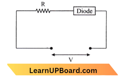
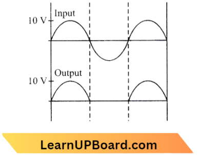
Question 27. If in a p-n junction, a square input single of 10 V is applied as shown in the given figure: Then the output across RL will be:
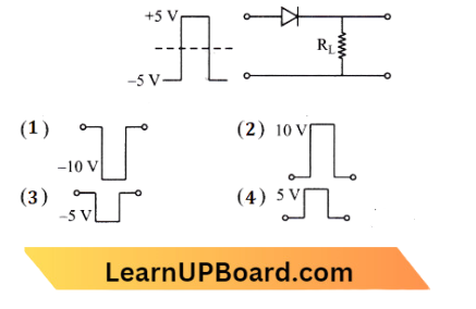
Answer: 4.
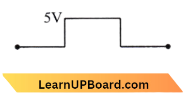
Because of + 5 V, it supports the forward bias of the diode and blocks the 5 V.
Question 28. In the given figure a diode D is connected to an external resistance R = 100 Ω and an E.M.F. of 3.5 V. If the barrier potential developed across the diode is 0.5 V, the current in the circuit will be:
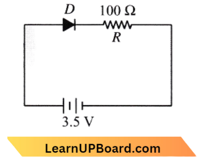
- 30 mA
- 40 mA
- 20 mA
- 35 mA
Answer: 1. 30 mA
According to the question,
External resistance, R=100 \(\Omega\)
emf=3.5 V
Potential difference on
R, \(V_R =3.5 V-0.5 \mathrm{~V}=3 \mathrm{~V}\)
Current I =\(\frac{V_R}{R}=\frac{3}{100}=0.03 \mathrm{~A}\)
= 30 mA
NEET Physics MCQs
Question 29. The given graph represents V-I characteristics for semiconductor devices. Which of the following statements is correct?
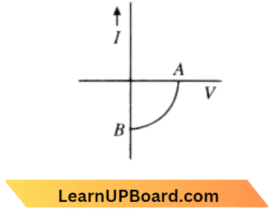
- It is V-I characteristics to the solar cell where point A represents open circuit voltage and point B short circuit current
- It is for a solar cell and points A and B represent open circuit voltage and current respectively
- It is for a photodiode and points A and B represent open circuit voltage and current respectively
- It is for an LED and points A and B represent open circuit voltage and short circuit current respectively
Answer: 1. It is V-I characteristics of solar cells where point A represents open circuit voltage and point B short circuit current
Question 30. The barrier potential of the p-n junction depends on:
- Type of semiconductor material
- Amount of doping
- Temperature
Which of the following is correct?
- (1) and (2) only
- (2) only
- (2) and (3) only
- (1) (2) and (3)
Answer: 4. (1) (2) and (3)
The barrier potential of a p-n junction depends on:
(1) Type of Semiconductor method: The potential barrier for a silicon p-n junction is 0.7 V at room temperature while for a generation p-n junction is 0.3 V.
(2) Amount of doping: Due to the difference in concentration, electrons diffuse from the n-side to the p-side and holes diffuse from the ft-side to the p-side and holes diffuse from the p-side to the n-side.
(3) Temperature: According to the temperature, the number of majority and minority carriers depends minority will also change
NEET Physics MCQs
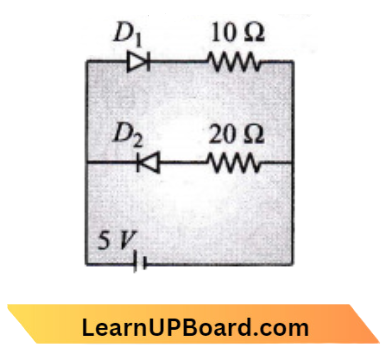
Question 31. Two ideal diodes are connected to a battery as shown in the circuit. The current supplied by the battery is:
- 0.75 A
- zero
- 0.2s A
- 0.5 A
Answer: 4. 0.5 A
Here \(D_1\) is at forward bias and \(D_2\) is at reverse bias, current flows only in \(D_1\). Then the diagram shows the Current flowing in the battery:
∴ \(\mathrm{I}=\frac{V}{R}=\frac{5 V}{10 \Omega}=0.5 \mathrm{~A}\)
Question 32. In the following figure, the diodes, which are forward-biased, are:
- 3 only
- 3 and 1
- 2 and 4
- 1, 2, and4
Answer: 2. 3 and 1
(1) and (3) both are in forward bias for forward bias p-type should be higher potential and in n-type at lower potential.
Class 12 Semiconductor MCQs
Question 33. In half wave rectification, if the input frequency is 60 Hz, then the output frequency would be:
- Zero
- 30 Hz
- 60 Hz
- 120 Hz
Answer: 3. 60 Hz
For half-wave rectification, the frequency remains the same as 60 Hz.
Question 34. forward biased diode is:
Answer: 1.
A diode is bound to be forward biased if if-type semi conducts of the p-n junction is at high potential w.r.t. n-type semiconductor of the p-n junction. It is so for the circuit (a).
Question 35. On the diodes shown in the following diagrams, which one is reverse biased:
Answer: 3.
A diode is at reverse bias if the p-side of the semiconductor of the p-n junction is at low potential w.r.t. n-type semiconductor of the p-n junction.
Class 12 Semiconductor MCQs
Question 36. Reverse bias applied to a junction diode:
- Lowers of the potential barrier
- Raises the potential barrier
- Increases the majority carrier’s current
- Increases the minority carrier’s current
Answer: 2. Raises the potential barrier
Reverse bias increases the potential barrier.
Question 37. For the given circuit of the p-n junction diode which is correct?
- In forward bias the voltage across R is V.
- In reverse bias the voltage across R is V.
- In forward bias, the voltage across R is 2 V.
- In reverse bias, the voltage across R is 2 V.
Answer: 1. In forward bias the voltage across R is V.
Important MCQs on Semiconductor Devices NEET
Question 38. If the internal resistance of the cell is negligible, then the current flowing through the circuit is:
- 3/50 A
- 5/50 A
- 4/50 A
- 2/50 A
Answer: 2. 5/50 A
Diode \(D_1\) is forward biased in the circuit, while diode \(D_2\) is reverse biased. As a result, no current flows via the \(D_2\)-containing arm, whereas all current flows through the \(D_1\)-containing arm.
Thus, current flowing through the circuit is I=\(\frac{V}{R_{e q}}=\frac{5}{20+30}=\frac{5}{20} \mathrm{~A}\)
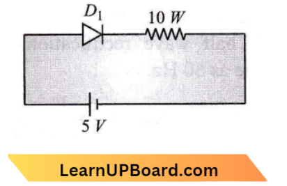
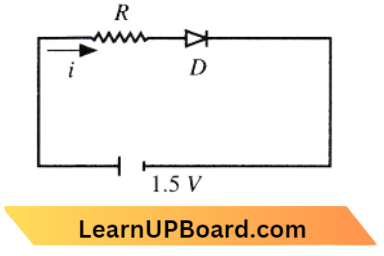
Question 39. A semiconducting device is connected in a series in a circuit with a battery and a resistance. A current is allowed to pass through the circuit. If the polarity of the battery is reversed, the current drops to almost zero. The device may be:
- P-n junction
- An intrinsic semiconductor
- A p-type semiconductor
- An n-type semiconductor
Answer: 1. P-n junction
We have, the current in a p-n junction on the order of milli-ampere in forward biasing and on the order of micro-ampere in reverse biasing (negligible). As a result, the device is a p-n junction.
Question 40. The diode used in the circuit shown in the figure has a constant voltage drop of 0.5 V at all currents and a maximum power rating of 100 milliwatts. What should be the value of the resistor R, connected in series with the diode, for obtaining maximum current l?
- 200
- 6.67
- 5
- 1.5
Answer: 3. 5
We have, current in the circuit,
i =\(\frac{P}{V_d}=\frac{100 \times 10^{-3}}{0.5}\)
=200\( \times 10^{-3} \mathrm{~A}\)
The voltage across resistance R,
⇒ \(V^{\prime}=1.5-0.5=1.0 \mathrm{~V}\)
Thus, resistance R =\(\frac{V^{\prime}}{I} \)
= \(\frac{1}{200 \times 10^{-3}}=5 \Omega\)
Important MCQs on Semiconductor Devices NEET
Question 41. In half wave rectification, if the input frequency is 60 Hz, then the output frequency would be:
- Zero
- 30 Hz
- 60 Hz
- 120 Hz
Answer: 3. 60 Hz
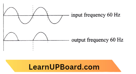
For half-wave rectification, the frequency remains the same as 60 Hz.
Question 42. The peak voltage in the output of a half-wave diode rectifier fed with a sinusoidal signal without a filter is 10 V. The D.C. component of the output voltage is:
- \(\frac{10}{\sqrt{2}} V\)
- \(\frac{10}{\pi} \mathrm{V}\)
- \(10 \mathrm{~V}\)
- \(\frac{20}{\pi} V\)
Answer: 2. \(\frac{10}{\pi} \mathrm{V}\)
∴ \(V_a=\frac{V_m}{\pi}=\frac{10}{\pi} \mathrm{V}\)
Question 43. If a full wave rectifier circuit is operating from 50 Hz mains, the fundamental frequency in the ripple will be:
- 25 Hz
- 50 Hz
- 70.7 Hz
- 100 Hz
Answer: 4. 100 Hz
In a full wave rectifier, the fundamental frequency in ripple is twice of input frequency.
Question 44. Consider the following statements (1) and (2) and identify the correct answer:
1. A zener diode is connected in reverse bias when used as a voltage regulator.
2. The potential barrier of the p-n junction lies between 0.1 V to 0.3 V.
- (1) and (2) both are correct
- (1) and (2) both are incorrect
- (1) is correct and (2) is incorrect
- (1) is incorrect but (2) is correct
Answer: 3. (1) is correct and (2) is incorrect
When the zener diode is forward biased, it behaves like an ordinary diode and when reverse biased, it will be a voltage stabilizer. Also, at room temperature, the voltage across the depletion layer for silicon is about 0.6- 0.7 V, and for germanium is about 0.3- 0.35 V.
PN Junction MCQs for NEET
Question 45. An LED is constructed from a p-n junction diode using Ga As P. The energy gap is 1.9 eV. The wavelength of the light emitted will be equal to:
- \(10.4 \times 10^{-26} \mathrm{~m}\)
- 654 nm
- \(654 Ål\)
- \(654 \times 10^{-11} \mathrm{~m}\)
Answer: 2 . 654 nm
The energy of light of wavelength \(\lambda\) is given by,
E =h v=\(\frac{h c}{\lambda}\)
⇒ \(\lambda =\frac{h c}{E}\)
Here h= Planck’s constant =6.63 \(\times 10^{-34} \mathrm{~J}.s.\)
c= speed of light =3 \(\times 10^8 \mathrm{~m} / \mathrm{s}\)
⇒ \(\mathrm{E}= energy gap =19 \mathrm{eV}\)
= \(1.9 \times 10^6 \times 10^{-19} \mathrm{~J}\)
Substituting the given values in Eq. (1), we get
⇒ \(\lambda =\frac{6.63 \times 10^{-34} \times 3 \times 10^8}{1.9 \times 1.6 \times 10^{-19}}\)
=6.54 \(\times 10^{-7} \mathrm{~m} \approx 654 \mathrm{~nm}\)
Thus, the wavelength of light emitted from LED will be 654 nm
Question 46. A Zener diode, having a breakdown voltage equal to 15 V is used in a voltage regulator circuit shown in the figure. The current through the diode is:
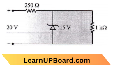
- 10 mA
- 15 mA
- 20 mA
- 5mA
Answer: 4. 5mA
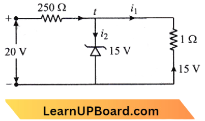
The actual diagram becomes
for 1 \(\mathrm{~K} \Omega, i_1=\frac{15}{1}=15 \mathrm{~mA}\)
for 250 \(\Omega,i_{250}=\frac{20-15}{250}=\frac{5}{250}\)
= \(\frac{20}{1000}=20 \mathrm{~mA}\)
∴ \(i_{\text {zener }}=20-15=5 \mathrm{~mA}\)
PN Junction MCQs for NEET
Question 47. A p-n photodiode is fabricated from a semiconductor with a band gap of 2.5 eV. It can detect a signal of wavelength:
- 6000 Å
- 4000 nm
- 6000 nm
- 4000 Å
Answer: 4. 4000 Å
Using de-Broglie equation
E =h v=\(\frac{h c}{\lambda} \)
⇒ \(\lambda =\frac{h c}{E}=\frac{6.6 \times 10^{-34} \times 3 \times 10^8}{2.5 \times 1.6 \times 10^{-19}}\)
=5000Å
As 4000 \(Å <5000 Å\)
The signal of wavelength is 4000 Å can be detected by the photodiode.
Question 48. A p-n photodiode is made of a material with a band gap of 2.0 eV. The minimum frequency of the radiation that can be absorbed in the material is nearly:
- \(10 \times 10^{14} \mathrm{~Hz}\)
- \(5 \times 10^{14} \mathrm{~Hz}\)
- \(1 \times 10^{14} \mathrm{~Hz}\)
- \(20 \times 10^{14} \mathrm{~Hz}\)
Answer: 2. \(5 \times 10^{14} \mathrm{~Hz}\)
The frequency corresponding to 2 eV is given by, E =h v
2 \(\times 1.6 \times 10^{-19} =66 \times 10^{-36} \times v \)
v =\(\frac{3.2 \times 10^{19}}{6.0+10^{-34}}=5 \times 10^{14} \mathrm{~Hz}\)
Question 49. Zener diode is used for:
- Amplification
- Rectification
- Stabilization
- Producing oscillations in an oscillator
Answer: 3. Stabilisation
The Zener diode is used for stabilization while the p-n junction divide is used for notification.
PN Junction MCQs for NEET
Question 50. In a p-n junction photocell, the value of the photo electromotive force by monochromatic light is proportional to:
- The barrier voltage at the p-n junction
- The intensity of the light falling on the cell
- The frequency of the light falling on the cell
- The voltage applied at the p-n junction
Answer: 2. The intensity of the light falling on the cell
In a p-n junction photocell, the value of the photo electromotive force produced by monochromatic light is proportional to the intensity of the light falling on the cell.
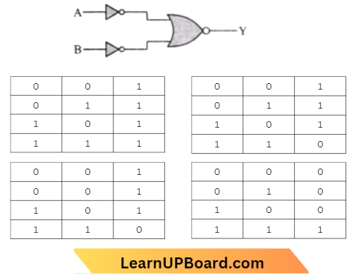
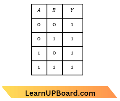
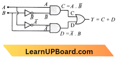
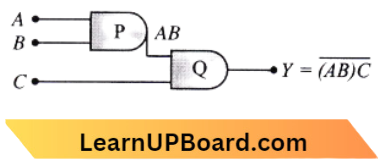
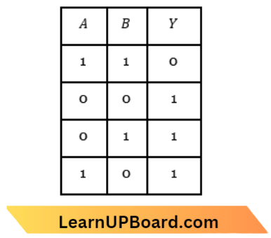
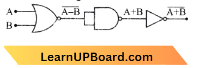
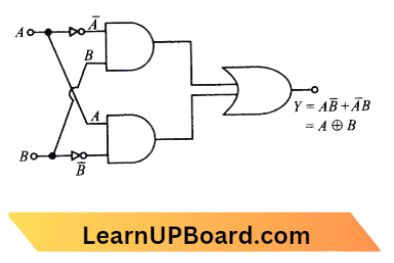
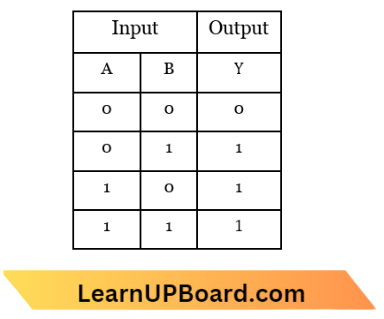
Question 51. The truth table for the given logic circuit is:
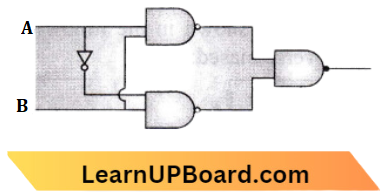
The Truth Table For The Given Logic Circuit Is:
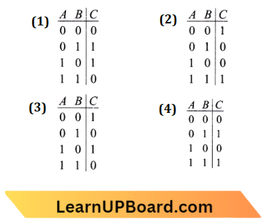
Answer: 3.
The output of the given circuit,
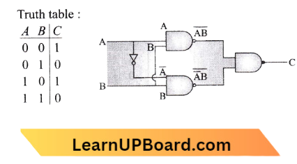
C=\(\overline{A B}+\overline{\bar{A} B} \)
C=\(\bar{A}+\bar{B}+\overline{\bar{A}}+\bar{B}\)
⇒ \(\mathrm{C}=\bar{A}+\bar{B}+A+\bar{B} \)
∴ \(\mathrm{C}=\overline{\mathrm{B}}\)
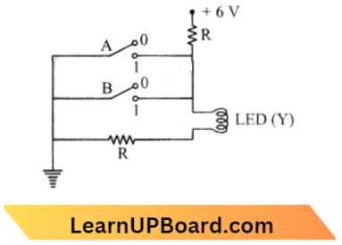
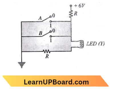
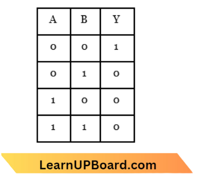
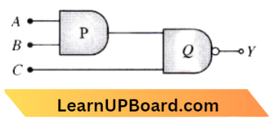
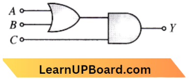
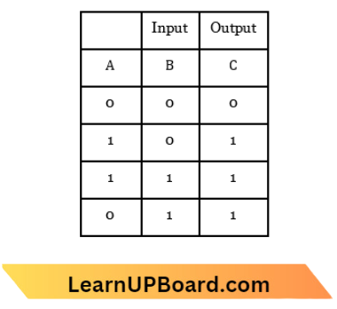
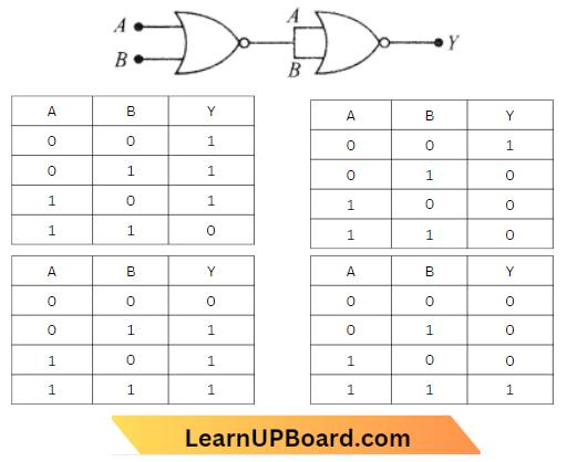
Question 52. For the given circuit, the input digital signals are applied at terminals A, B, and C. What would be the output at the terminal?
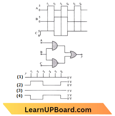
Answer: 3.
So, the output at y is high (1) i.e. V0 = 5 V.
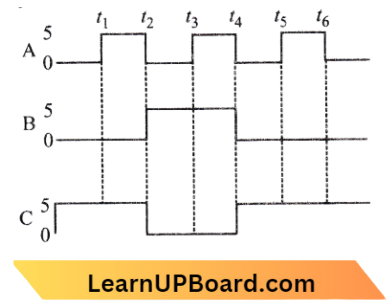
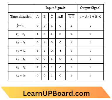
Hence, option (3) is correct
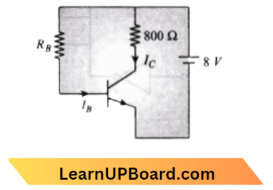
Question 53. An n-p-n transistor is connected in a common emitter configuration (see figure) in which the collector voltage drop across load resistance (800 Ω) connected to the collector circuit is 0.8 V. The collector current is:
- 2 mA
- 0.1 mA
- 1 mA
- 0.2 mA
Answer: 3. 1 mA
Given
An n-p-n transistor is connected in a common emitter configuration (see figure) in which the collector voltage drop across load resistance (800 Ω) connected to the collector circuit is 0.8 V.
From the given circuit diagram,
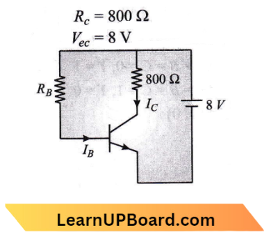
⇒ \(R_c =800 \Omega\)
⇒ \(V_{e c} =8 \mathrm{~V}\)
Now, the voltage drop across \(R_C,\)
⇒ \(I_C R_C =0.8 \)
∴ \(I_C =\frac{0.8}{R_C}=\frac{0.8}{800} 10^{-3} \mathrm{~A}=1 \mathrm{~mA} \).
PN Junction MCQs for NEET
Question 54. For transistor action, which of the following statements is correct?
- Base, emitter, and collector regions should have the same size.
- Both, the emitter junction as well as the collector junction are forward-biased.
- The base region must be very thin and lightly doped.
- Base, emitter, and collector regions should have the same doping concentrations.
Answer: 3. The base region must be very thin and lightly doped.
For transistor action, the base region must be very thin and lightly doped.
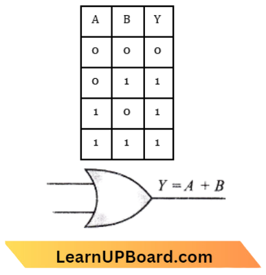
Question 55. Which of the following gates is called a universal gate?
- OR gate
- AND gate
- NAND gate
- NOR gate
Answer: 3. NAND gate
NAND and NOR gates are universal gates.
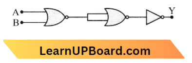
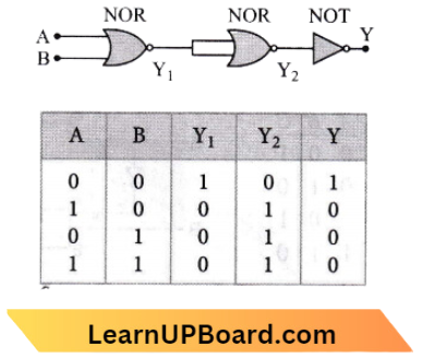
Question 56. For the logic circuit shown, the truth table is
Answer: 4.
The logic gate becomes,
Here, Y=\(\overline{\bar{A}+\bar{B}}=\overline{\bar{A}}+\overline{\bar{B}}\)
This Is In Option 4
PN Junction MCQs for NEET
Question 57. The correct Boolean operation represented by the circuit diagram drawn is
- OR
- NAND
- NOR
- AND
Answer: 4. AND
From the given logic circuit LED will glow when the voltage across the LED is high.
This is the output of the NAND gate.
Question 58. The circuit diagram shown here corresponds to the logic gate:
- NOR
- OR
- AND
- NAND
Answer: 1. NOR
From the circuit diagram given below, it can be seen that the current will flow to the ground if any of the switches are closed.
Thus, the truth table for the circuit diagram can be formed as the circuit diagram is given a solution.
The output (Y) is equivalent to that of the NOR gate.
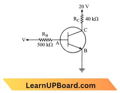
Question 59. In the circuit shown in the figure, the input voltage \(V_{i}=0\) is 20 V, \(V_{B E}=0\), and \(V_{C E}=0\). The values of \(I_B, I_C\)and \(\beta\) given by:
- \(I_{\mathrm{B}}=20 \mu \mathrm{A}, I_{\mathrm{c}}=5 \mathrm{~mA}, \beta=250\)
- \(I_{\mathrm{B}}=25 \mu \mathrm{A}, I_{\mathrm{c}}=5 \mathrm{~mA}, \beta=200\)
- \(I_{\mathrm{B}}=40 \mu \mathrm{A}, I_{\mathrm{c}}=5 \mathrm{~mA}, \beta=250\)
- \(I_{\mathrm{B}}=40 \mu \mathrm{A}, I_{\mathrm{c}}=5 \mathrm{~mA}, \beta=125\)
Answer: 4. \(I_{\mathrm{B}}=40 \mu \mathrm{A}, I_{\mathrm{c}}=5 \mathrm{~mA}, \beta=125\)
From question, \(V_{B E} =0 \mathrm{~V} \)
⇒ \(V_{C B} =0 \mathrm{~V}\)
⇒ \(V_i =20 \mathrm{~V}\)
and Applying Kirchhoff’s law,
⇒ \(V_I=I_B R_B+V_{B E}\)
Putting the values,
20 =\(I_B \times\left(500 \times 10^3\right)+0\)
⇒ \(I_B=40 \times 10^{-6}=40 \mu \mathrm{A}\) → Equation 1
Similarly, \(V_{C C}=l_C R_C+V_{E C}\)
Again, putting the values
20=\(I_C \times\left(4 \times 10^3\right)+0\)
⇒ \(I_C=5 \times 10^{-3}=5 \mathrm{~mA}\)
Again we know that current \(\beta=\frac{I_C}{I_B}\) → Equation 2
⇒ \(\beta =\frac{5 \times 10^{-3}}{40 \times 10^{-6}}\)
=\(0.125 \times 10^3\)=125
∴ \(I_B=40 \mu \mathrm{A}, I_C=5 \mathrm{~mA}, \beta\)=125
Chapter-Wise Physics MCQs for NEET
Question 60. In a common emitter transistor amplifier, the audio signal voltage across the collector is 3 V. The resistance of the collector is 3Ω). If the current gain is 100 and the base resistance is 2Ω), the voltage and power gain of the amplifier are;
- 200 and 1000
- 15 and 200
- 150 and 15000
- 20 and 2000
Answer: 3. 150 and 15000
Given
In a common emitter transistor amplifier, the audio signal voltage across the collector is 3 V. The resistance of the collector is 3Ω). If the current gain is 100 and the base resistance is 2Ω),
Current gain,\((\beta)\)=100
Voltage gain, \(\left(A_V\right)=\beta \frac{R_c}{R_b}=100 \times \frac{3}{2}\)=150
Now Powers gain, P =\(A_V \cdot b\)
=150 \(\times 100\)=15000
Question 61. In the combination of the following gates, the output Y can be written in terms of inputs A and B as:
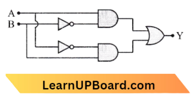
- \(\overline{\mathrm{A} \cdot \mathrm{B}}+\mathrm{A} \cdot \mathrm{B}\)
- \(\mathrm{A} \cdot \overline{\mathrm{B}}+\overline{\mathrm{A}} \cdot \mathrm{B}\)
- \(\overline{\mathrm{A} . \mathrm{B}}\)
- \(\overline{\mathrm{A}+\mathrm{B}}\)
Answer: 2. \(\mathrm{A} \cdot \overline{\mathrm{B}}+\overline{\mathrm{A}} \cdot \mathrm{B}\)
The combined figures for inputs and outputs are given below:
Question 62. The given electrical network is equivalent to:
- AND gate
- OR gate
- NOR gate
- NOT gate
Answer: 3. NOR gate
Truth Table Is:
Y→ NOR – gate
Question 63. A n-p-n transistor is connected in a common emitter configuration in a given amplifier. A load resistance of 800 Ω is connected in the collector circuit and the voltage drop across it a 0.6 V. If the current amplification factor is 0.96 and the input resistance of the circuits is 192 Ω, the voltage gain and the power gain of the amplifier will respectively be:
- 3.69,3.84
- 4.4
- 4,3.69
- 4,3.84
Answer: 4. 4,3.84
Here, \(R_0 =800 \Omega, R_i=192 \Omega\)
⇒ \(\beta\) =0.96
Voltage gain =0.96 \(\times \frac{800}{192}\)=4
Power gain =0.96 \(\times 4\)=3.84
Chapter-Wise Physics MCQs for NEET
Question 64. For the CE transistor amplifier, the audio signal voltage across the collector resistance of 2 kD. is 4 V. If the current amplification factor of the transistor is 100 and the base resistance is 1 kfi then the input signal voltage is:
- 100 mv
- 20 mV
- 30 mV
- 15 mV
Answer: 2. 20 mV
We Know The Formula,
Voltage amplification,
⇒ \(A_V=\beta \frac{\mathrm{R}_{\text {out }}}{R_n}=\frac{\left(\mathrm{V}_{\text {out }}\right)_{A C}}{\left(V_{\text {in }}\right)_{A C}}\)
Where,\( R_{\text {out }}\) =2 K W= collector resistance
B =100=amplification factor
⇒ \(R_n =1 \mathrm{KW}\)= Base resistance
V =4 \(\mathrm{~V}\)= output voltage
putting these values in equation (1)
⇒ \(A_V=\beta \frac{R_{\text {out }}}{R_n}=100 \times \frac{2 \mathrm{~K} \Omega}{1 \mathrm{~K} \Omega}\)
⇒ \(A_V=200\)
Now,\( A_V=\frac{\left(\mathrm{V}_{\text {out }}\right)_{\mathrm{AC}}}{\left(\mathrm{V}_{\text {in }}\right)_{\mathrm{AC}}}\)
∴ \(\left(V_{i n}\right)_{A C}=\frac{4}{200}=20 \mathrm{mV} \)
Question 65. What is the output Y in the following circuit, when all the three inputs A, B, C are first 0 and then 1?
- 0, 1
- 0, 0
- 1,0
- 1, 1
Answer: 3. 1,0
for A=B = C = 0, Y=1
for A = B = C=1,Y=0
Y is(1,0)
Question 66. To get output 1 for the following circuit, the correct choice for the input is:

- A=1,B=0,C=0
- A=1,B=1,C=0
- A=1,B=0,C=1
- A=0,B=1,C=0
Answer: 3. A=1,B=0,C=1
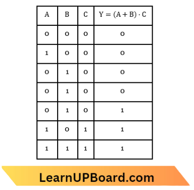
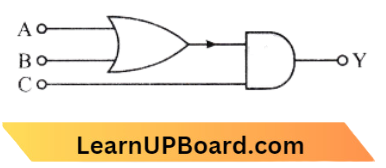
From the figure, the boolean algebra expression of the logic gate is
Y = (A+B).C
Consider different cases :
Case (1): If = 0,5 = 0, C= 0
7 = (6 + 0).0 = 0
Case (2): If A = 1 B = 1 C=0
Y= 1.0 => Y=0
Case (3): If A( = 1 5 = 0 C = 1
Y = (1 + o),1 = 1.1 = Y=1
Case (4): If ÿ = 05 = 1 C = 0
7 = (1 + 1). 0 = 0
From the above four cases, it is confirmed that output 1 is obtained in option (3)
A =1,5 = 0, C= 1
Chapter-Wise Physics MCQs for NEET
Question 67. The input signal given to a CE amplifier having a voltage v gain of 150 is \(V_1=2 \cos \left(15 t+\frac{\pi}{3}\right)\). The corresponding output signal will be:
- \(300 \cos \left(15 t+\frac{\pi}{3}\right)\)
- \(75 \cos \left(15 t+\frac{2 \pi}{3}\right)\)
- \(2 \cos \left(15 t+\frac{5 \pi}{3}\right)\)
- \(300 \cos \left(15 t+\frac{4 \pi}{3}\right)\)
Answer: 4. \(300 \cos \left(15 t+\frac{4 \pi}{3}\right)\)
We know that \(V_0=\beta V_i\) and phase difference of \(\pi\)
⇒ \(V_0 =150 \times 2 \cos \left(15 t+\frac{\pi}{3}+\pi\right)\)
=300 \(\cos \left(15 t+\frac{4 \pi}{3}\right)\)
Question 68. Which logic gate is represented by the following combination of logic gates?
- OR
- NAND
- AND
- NOR
Answer: 3. AND
Its output Y shows that it is an AND-Gate.
Question 69. In a common emitter (CE) amplifier having a voltage gain of G, the transistor used has a transconductance of 0.03 mho and a current gain of 25. If the above transistor is replaced with another one with transconductance 0.02 mho and current gain 20, the voltage gain will:
- 2/3 G
- 1.5G
- 1/3 G
- 5/4 G
Answer: 1. 2/3 G
Voltage gain,\(\mathrm{A}_{\mathrm{V}}=\beta \times \frac{R_{\text {out }}}{R_{\text {in }}}\)
Transconductance,
⇒ \(g_m =\frac{\beta}{R_{i n}} \text { or } R_{\text {in }}=\frac{\beta}{g_m}\)
⇒ \(\mathrm{A}_{\mathrm{V}} =g_m \mathrm{R}_{\text {out }}\)
For 1st Case, \(\mathrm{G} =0.03 \mathrm{R}_{\text {out }}\)
For 2nd Case, \(G^{\prime} =0.02 \mathrm{R}_{\text {out }} \)
Now, \(\frac{G^{\prime}}{G^0} =\frac{2}{3} or G^{\prime}=\frac{2}{3} G\)
Chapter-Wise Physics MCQs for NEET
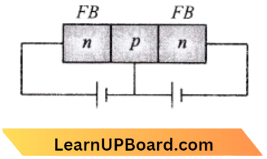
Question 70. One way in which the operation of an n-p-n transistor differs from that of ap-n-p.
- The emitter junction injects minority carriers into the base region of the p-n-p.
- The emitter junction injects minority carriers into the base region of the p-n-p.
- The emitter injects holes into the base of n-p-n.
- The emitter junction is reversed-biased in n-p-n.
Answer: 2. The emitter junction injects minority carriers into the base region of the p-n-p.
The emitter injects holes into the base of the p-n-p and electrons into the base region of n-p-n.
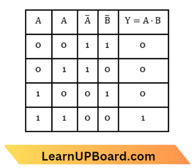
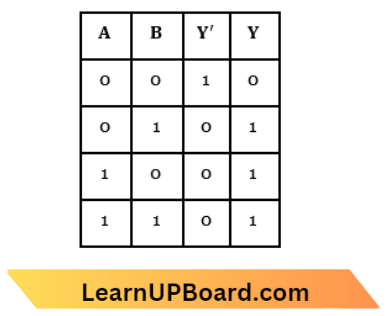
Question 71. The output (X) of the logic circuit shown in the figure will be:
- \(\mathrm{X}=\overline{\overline{\mathrm{A}}} \cdot \overline{\mathrm{B}}\)
- \(\mathrm{X}=\overline{\mathrm{A} . \mathrm{B}}\)
- \(X=A \cdot B\)
- \(\mathrm{X}=\overline{\mathrm{A}+\mathrm{B}}\)
Answer: 3. \(X=A \cdot B\)
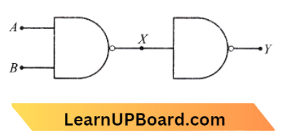
∴ \(\mathrm{X}=\overline{\mathrm{AB}}=\mathrm{A} \cdot \mathrm{B}\) i.e. And gate.
Question 72. The output from a NAND gate is divided into two in parallel and fed to another NAND gate. The resulting gate is a:
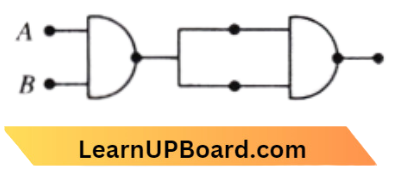
- AND gate
- NOR gate
- OR gate
- NOT gate
Answer: 1. AND gate
Output is C=\(\overline{\bar{A} \cdot B}=A \cdot B \rightarrow\) This is AND-gate
Logic Gates MCQs for NEET
Question 73. In a CE transistor amplifier, the audio signal voltage across the collector resistance of 2 kΩ is 2 V. If the base resistance is 1 kΩ and the current amplification of the transistor is 100, the input signal voltage is:
- 0.1 V
- 1.0 V
- l mV
- 10 mV
Answer: 4. 10 mV
It is given that,
⇒ \(\beta =100=\frac{\mathrm{I}_{\mathrm{C}}}{\mathrm{I}_{\mathrm{B}}} \)
⇒ \(R_{\mathrm{C}} =2 \mathrm{k} \Omega\)
⇒ \(V_{\mathrm{L}} =2 \mathrm{~V} \)
⇒ \(R_B =1 \mathrm{k} \Omega \)
⇒ \(I_C =\frac{V_C}{R_C}=\frac{2}{2}=1 \mathrm{~mA} \rightarrow\)collector current
⇒ \(I_B =\frac{V_B}{R_B}=\frac{V_B}{I}=\mathrm{V}_{\mathrm{B}} \mathrm{mA} \rightarrow\) Base current
⇒ \(\beta =100=\frac{1}{\mathrm{~V}_{\mathrm{B}}}\)
⇒ \(V_B =\frac{1}{100}=0.01 \mathrm{~V}=10^{-2} \mathrm{~V}\)
∴ \(V_B =10 \mathrm{mV}\)
Question 74. Transfer characteristic [output voltage (V0) vs input •voltage (V1)] for a base-biased transistor in CE configuration is as shown in the figure. For using a transistor as a switch, it is used:
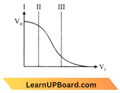
- In region 3
- Both in the region (1) and (3)
- In region 2
- In region 1
Answer: 2. Both in regions (1) and (3)
For using a transistor as a switch it is used in
(1) cut off state
(2) Saturation state only.
They are both in region (1) and (2)
Logic Gates MCQs for NEET
Question 75. The input resistance of a silicon transistor is 100 Ω. Base current is changed by 40 μA which results in a change in collector current by 2 mA. This transistor is used as a common-emitter amplifier with a load resistance of 4kμ. The voltage gain of the amplifier is:
- 2000
- 3000
- 4000
- 1000
Answer: 1. 2000
Current gain, \(\beta=\frac{\Delta \mathrm{I}_e}{\mathrm{I}_\beta}=\frac{2 \times 10^{-3}}{40 \times 10^{-6}}\)
⇒ \(\beta\)=50
∴ Voltage gain, \(A_{\mathrm{V}}=\beta\left(\frac{\mathrm{R}_{\text {out }}}{\mathrm{R}_{\text {in }}}\right)\)=2000
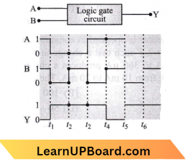
Question 76. The figure shows a logic circuit with two inputs A and B and the output C. The voltage waveforms across A, B, and C are as given. The logic circuit gate is:
- OR gate
- No gate
- AND gate
- NAND gate
Answer: 1. OR gate
From the given logic gate the truth table is :
This table is the table of the ‘OR’ gate.
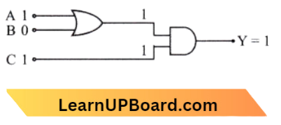
Question 77. To get output Y = 1 in the given circuit which of the following inputs will be correct:
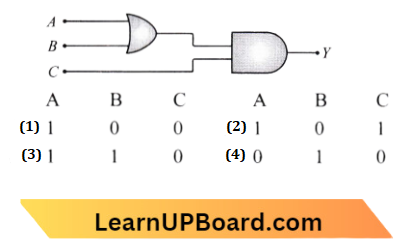
Answer: 2.
Question 78. A transistor is operated in a common emitter configuration at VQ = 2 V such that a change in the base current from 100 μA to 300 μA produces changes in the collector current from 10 mA to 20 mA. The current gain is:
- 75
- 100
- 25
- 50
Answer: 4. 50
⇒ \(\beta =\frac{\Delta I_C}{\Delta I_B} \)
= \(\frac{(20-10) \times 10^{-3}}{(300-100) \times 10^{-6}}\)=50
Logic Gates MCQs for NEET
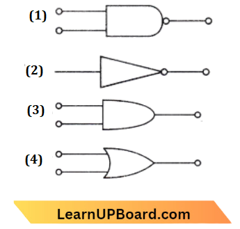
Question 79. The symbolic representation of four logic gates is shown as:
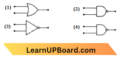
Pick out which ones are for AND, NAND, and NOT gates respectively.
- (3), (2), and (1)
- (3), (2), and (4)
- (2), (4), and (3)
- (2), (3), and (4)
Answer: 3. (2), (4) and (3)
In the given figure
(1) → OR-gate (2) → AND-gate
(3) → NOT-gate (4) → NAND-gate
Hence option (C) is correct
Question 80. A common emitter amplifier has a voltage gain of 50, an input impedance of 100 Ω, and an output impedance of 200 Ω. The power gain in the amplifier is:
- 500
- 1000
- 1250
- 50
Answer: 3. 1250
We know that, voltage gain =\(\beta \times\) impedance gain
50 =\(\beta \times \frac{200}{100} \)
= 25
Power gain =\(\beta^2 \times\) impedance gain
= \((25)^2 \times \frac{200}{100}\)=1250
Question 81. For transistor action:
- Base, emitter, and collector regions should have similar sizes and doping concentrations.
- The base region must be very thin and lightly doped.
- The emitter base junction is forward and the base collector junction is reverse-biased.
- Both the emitter-base junction as well as the base-collector junction are forward-biased
Which one of the following pairs of statements is correct?
- (4) and (1)
- (1) and (2)
- (2) and (3)
- (3) and (4)
Answer: 3. (2) and (3)
For transistor action
(1) The base region must be very thin and lightly doped.
(2) The emitter-base is forward-biased and the base-collector junction is reverse-biased.
Question 82. To get output Y = 1 from the circuit shown below, the input must be:
Answer: 4.
Gate 1 OR-gate, \(y^{\prime}=\mathrm{A}+\mathrm{B}\)
Gate 2 AND-gate, \(y=y^{\prime}\). c
∴ \(\mathrm{A}=1, \mathrm{~B}=0, \mathrm{C}=0 \Rightarrow \)Y=1
Question 83. The following figure shows a logic gate circuit with two inputs A and B and output Y. The voltage waveforms of A, B, and Y are as given:
The logic gate is:
- NOR gate
- OR gate
- AND gate
- NAND gate
Answer: 4. NAND gate
The truth table for logic gate i.e.
This is NAND-gate
Logic Gates MCQs for NEET
Question 84. The device that can act as a complete electronic circuit is:
- Junction diode
- Integrated circuit
- Junction transistor
- Zener diode
Answer: 2. Integrated circuit
The device that can act as a complete electronic circuit is an integrated circuit.
Question 85. A transistor is operated in a common-emitter configuration at Vc=2 volt such that a change in the base current from 100 μA to 200 μA produces changes in the collector current from 5 mA to 10 mA. The current gain is:
- 75
- 100
- 150
- 50
Answer: 4. 50
According to the question
For the transistor, \(I_E=I_B+I_C \)
⇒ \(I_E\)= Emitter current
⇒ \(I_B\)= case current =100 \(\mu \mathrm{A} \)
⇒ \(I_C\)= Collector current =5 \(\mathrm{~mA}\)
and current gain, \(\beta=\frac{\Delta I_C}{\Delta I_B}\)
∴ \(\beta=\frac{5 \times 10^{-3}}{100 \times 10^{-6}}\)=50
Question 86. The symbolic representation of four logic gates:
The logic symbols for OR, NOT, and NAND gates are respectively;
- 3, 4, 2
- 4, 1, 3
- 4, 2, 1
- 1, 3, 4
Answer: 3. 4, 2, 1
(1) NAND Gate
(5) NOT Gate
(4) OR Gate
The correct options would be (3).
Logic Gates MCQs for NEET
Question 87. The voltage gain of an amplifier with 9% negative feedback is 10. The voltage gain without feedback will be:
- 90
- 10
- 1.25
- 100
Answer: 4. 100
Voltage gain with feedback is
⇒ \(A_{v f}=\frac{A_V}{1+\beta A_V}\) → Equation 1
Where, \(A_V\)= voltage gain without feedback and \(\beta\)= negative feedback
From the question,
⇒ \(A_{v f}=10, \beta=9 \%=\frac{9}{100}\)
Putting in eq. (i)
10=\(\frac{A_V}{1+\frac{9}{100} A_V}\)
Putting in eq. (1)
10 =\(\frac{A_V}{1+\frac{9}{100} A_V}\)
or \(10+\frac{9}{10} \mathrm{~A}_{\mathrm{V}} =A_V\)
0.1 A_V =10
∴ \(A_V\) =100
Question 88. For a transistor circuit, the base current is 10μA, and the collector current is 5.2 μA. Can this transistor circuit be used as an amplifier? Your answer must be supported with a proper explanation.
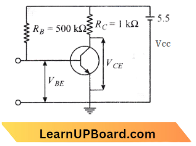
- 0.5 v
- 0.1 v
- 0.3 v
- 0 v
Answer: 3. 0.3 v
From the question,
⇒ \(V_{B E} =V_{C C}-I_B R_B \)
= 5.5-10 \(\times 10^{-6} \times 500 \times 10^3 \)
=0.5 \(\mathrm{~V}\)
⇒ \(V_{C E} =V_C-I_C R_C \)
=5.5-5.2 \(\times 10^{-3} \times 1 \times 10^3\)
=0.3 V
Both the E-B function and the C-E function are forward bias, they can not be used as an amplifier.
Question 89. The circuit is equivalent to:
- AND gate
- NAND gate
- NOR gate
- OR gate
Answer: 3. NOR gate
The output is of the NOR gate hence the combination will act as a NOR gate.
Logic Gates MCQs for NEET
Question 90. A common emitter amplifier has a voltage gain of 50, an input impedance of 100Ω, and an output impedance of 200 Ω. The power gain of the amplifier is:
- 1000
- 1250
- 100
- 500
Answer: 3. 100
Voltage gain =\((\beta)\left(\frac{\mathrm{R}_0}{\mathrm{R}_i}\right)\)=50
⇒ \(\beta=\frac{50 \times 100}{200}\)=25
Power gain =\((125)^2 \times \frac{200}{100} \)
= \((125)^2 \times \frac{200}{100} \)
= 625 \(\frac{200}{100}\)
= 1250
Question 91. In the following circuit, the output Y for all possible inputs A and B is expressed by the truth table.
Answer: 3.
∴ \(y^{\prime}=\overline{\mathrm{A}+\mathrm{B}}, y=p+e+v=\mathrm{A}+\mathrm{B}\)
Question 92. A transistor is operated in a common-emitter configuration at Vc= 2 volt such that a change in the base current from 100 μA to 200 μA produces changes in the collector current from 5 mA to 10 mA. The current gain is:
- 0.8 v
- 0.1 v
- 0.3 v
- 0 v
Answer: 4. 0 v
Current gain =\(\beta=\frac{\Delta I_C}{\Delta I_B}\)
=\(\frac{(10-5) \mathrm{mA}}{(150-100) \mu \mathrm{A}}=\frac{5 \times 10^{-3}}{50 \times 10^{-6}} \)
=100
Diode and Transistor Questions for NEET
Question 93. The following figure shows a logic gate circuit with two inputs A and B and the output C. The voltage waveforms of A, B, and C are as shown below:
The logic circuit gate is:
- OR Gate
- AND Gate
- NAND Gate
- NOR Gate
Answer: 2. AND Gate

The circuit is AND- gate
Question 94. The output of the OR gate is 1:
- If both inputs are zero
- If either of both inputs is 1
- Only if both inputs are 1
- If either input is zero
Answer: 2. If either of both inputs are 1
means if either or both inputs are 1.
Question 95. An-p-n transistor conducts when:
- Both collector and emitter are positive with respect to the base
- The collector is positive and the emitter is negative with respect to the base
- The collector is positive and the emitter is at the same potential as the base
- Both collector and emitter are negative with respect to the base
Answer: 2. Collector is positive and emitter is negative with respect to the base
In the active region Emitter base p-n function is in FB and the base collector p-n function is in RB.
Diode and Transistor Questions for NEET
Question 96. For transistor \(\frac{I_C}{I_{E_c}}=0.96\), then the current gain for common emitter configuration :
- 12
- 6
- 48
- 24
Answer: 4. 24
For the common emitter configuration, the current transfer ratio is,
⇒ \(\alpha =\frac{I_C}{I_B}\)=0.96
Current gain, =\(\frac{\alpha}{1-\alpha}\)
= \(\frac{0.96}{1-0.96}\)=24
Question 97. For which logic gate, the given truth table is shown?

- NAND
- XOR
- NOR
- OR
Answer: 1. NAND
It is a NAND-gate
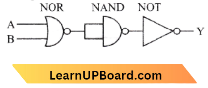
Question 98. The following diagram performs the logic function of
- OR gate
- AND gate
- XOR gate
- NAND gate
Answer: 2. AND gate
Let the output of the first NAND gate be chosen as X as shown in the diagram below.

Output of 1st NAND gate, X=\(\overline{A \cdot B}\)
Using De-Morgan’s theorem
⇒ \(\overline{A \cdot B}=\bar{A}+\bar{B}\)
So, X=\(\bar{A}+\bar{B}\)
Now, output of \(2^{\text {nd }}\) NAND gate,
Again, Y =\(\bar{X}=\overline{\bar{A}+\bar{B}} \)
⇒ \(\overline{\bar{A}+\bar{B}} =\bar{A} \cdot \bar{B}=A \cdot B\)
Y =A \(\cdot B\)
Hence, This is the AND gate’s logic function.
Question 99. If cr and B are current gains in common-base and common-emitter configurations of a transistor, then B is equal to:
- \(\frac{1}{\alpha}\)
- \(\frac{\alpha}{1+\alpha}\)
- \(\frac{\alpha}{1-\alpha}\)
- \(\alpha-\frac{1}{\alpha}\)
Answer: 3. \(\frac{\alpha}{1-\alpha}\)
The current gain in common-base configuration,
⇒ \(\alpha=\left(\frac{\Delta i_c}{\Delta i_e}\right)_{V_{c b}}\)
The current gain in common-emitter configuration,
Also, \(\beta=\left(\frac{\Delta i_c}{\Delta i_b}\right)_{v_\sigma}\)
Also, \(i_b =i_e-i_c\)
⇒ \(\Delta i_b =\Delta i_e-\Delta i_c\)
⇒ \(\beta=\frac{\Delta i_c}{\Delta i_b}=\frac{\Delta i_c}{\Delta i_e} \times \frac{\Delta i_e}{\Delta i_b}\)
⇒ \(\beta=\alpha \times \frac{\Delta i_e}{\Delta i_e-\Delta i_c}\)
⇒ \(\beta=\alpha \times \frac{1}{1-\frac{\Delta i_c}{\Delta i_e}}\)
∴ \(\beta=\frac{\alpha}{1-\alpha}\)
Diode and Transistor Questions for NEET
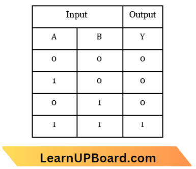
Question 100. The truth table given below represents
- AND gate
- NOR gate
- OR gate
- NAND gate
Answer: 4. NAND gate
A NAND gate gives output as 1 when either of the input signals is low, i.e., O, and gives output as 0 only when better the input signals are high, i.e., Hence the above truth table is for the NAND gate.
Thus, the NAND gate will give an output of 1
Question 101. The transfer ratio p of a transistor is 50. The input resistance of the transistor when used in the common emitter configuration is 1kΩ. The peak value of the collector. AC current for an AC input voltage of 0.01 V peak is:
- 100 μA
- 0.01 mA
- 0.25 mA
- 500 μA
Answer: 4. 500 pA
Input current or We have,
B current, \(i_{\mathrm{b}}=\frac{\Delta V_b}{R_b}=\frac{0.01}{10 \rho 0}=10^{-5} \mathrm{~A}\)
⇒ (\(\Delta V_b\) = input voltage; \(\Delta R_{\mathrm{b}}\) = base resistance)
Also Current gain, \(\beta=\frac{i_c}{i_b}\)
⇒ \(i_{\mathrm{c}}=\beta i_{\mathrm{c}}=50 \times 10^{-5} \mathrm{~A}\)
= \(500 \times 10^{-6} \mathrm{~A}=500 \mu \mathrm{A}\)
Question 102. The part of the transistor which is heavily doped to produce large number of majority carriers is:
- Emitter
- Base
- Collector
- Any of the above depending upon the nature of the transit
Answer: 1. Emitter
The transistor has three regions, namely emitter, base, and collector. The base is much thinner than the emitter, while the collector is wider than both. The emitter is heavily doped so that it can inject a large number of charge carriers (electrons or holes) into the base. The base is lightly doped and very thin, it passes most of the emitter-injected charge carriers to the collector. The collector is moderately doped.
Diode and Transistor Questions for NEET
Question 103. To use a transistor as an amplifier,
- The emitter-base junction is forward biased and the base-collector junction is reversed biased
- No bias voltage is required
- Both junctions are forward-biased
- Both junctions are revealed as biased
Answer: 1. The emitter-base junction is forward biased and the base-collector junction is reversed biased
A transistor is used as an amplifier in a common emitter (CE) configuration. In this configuration, the base-emitter junction is forward-biased and the collector-base junction is reverse-biased
Diode and Transistor Questions for NEET
Question 104. The following truth table corresponds to the logical gate
- NAND
- OR
- AND
- XOR
Answer: 2. OR
The given truth table shows that, if any or all of the inputs are high, then the output is high. The only method to get a low output is to set all of the inputs to zero. If any or all of the inputs are high, the OR gate’s output 1 is high. As a result, the tiris truth table is an OR gate truth table.